Sonata system
Sonata is a system for evaluating the usage of CHERIoT Ibex core as a microcontroller for embedded, IoT and Operational Technology applications. The system contain a number of peripherals (I2C, SPI, GPIO, PWM, UART, and DMA) and a CHERIoT enabled debug module along with the CHERIoT Ibex core itself.
It is designed for use on FPGA and specifically targets the Sonata FPGA board, but as the entire design (from example PCB to software) is open-source it can be run on any similar system.
This project is designed to look like a normal microcontroller in terms of usability, including SDK, examples, and normal capabilities such as debuggers. But underneath that the CHERIoT capabilities provides a high level of "default security" that simplifies designing embedded systems in a secure manner. You can see the complete documentation for the project, but note it is under active development so substantial improvements are to be made.
As this project is under active development the first full RTL release is not yet complete. We plan to release an updated image, together with instructions for uploading it to the board over USB, before the May 29th 2024 Hackathon event. This image will allow running CHERIoT-RTOS and will allow for general purpose software development.
Sonata is part of the Sunburst Project funded by UKRI / DSbD under grant number 107540.
Getting Started

If you have a Sonata board, you can jump to the Getting Started guide. This will walk you through plugging in the board, building example software, and programming the software. For more advanced usage, you can see a Reference Manual similar to what a normal microcontroller reference manual (peripherals, features, etc) and then see the FPGA development flow if you wish to modify the soft-core itself
You can also work with a simulated environment, see the simulator page. This simulates the entire soft-core in Verilator, allow you to develop both hardware (the FPGA) and software (running code) programs.
Documentation Intro
This documentation is built using mdBook. If you are reading this file in GitHub, you should instead see the pre-built documentation on the lowRISC Website which includes the full documentation.
If you'd like to build a copy of the documentation locally, see the Building Documentation page.
License
Unless otherwise noted, everything in the repository is covered by the Apache License, Version 2.0. See the LICENSE file for more information on licensing.
Getting started with Sonata Board
This guide helps you to get started with the Sonata board by building code with CHERIoT technology enabled. One more advanced feature of Sonata is you can adjust the number and type of peripherals included. This is described in the section FPGA Development, for this getting started guide you will use one of the default setups.
The Sonata board is a prototype board and is under active development. This documentation is in the process of being updated. We will be improving the getting started guide soon to allow for an easier way with developing against the boards.
Getting Started Steps
To get started with your Sonata board, there are three steps you'll need to do. First, head to the Sonata System Release Page where you'll find the latest releases.
- Program the RP2040 With the Latest firmware to get any bug fixes by entering bootloader mode & dragging the
rpi_rp2_v0.XX.uf2. - Get the latest FPGA image that corresponds with the software you are building. This requires you to just drag the new
.bitfile onto the SONATA drive that comes up when you plug in the board to your computer. - Install the software toolchain.
- Build the example code and download to the soft-core you loaded in step 1.
Follow along each of the following sections to complete these tasks.
Reloading the RP2040 USB Controller
Before plugging in your Sonata board, hold down the SW9 labelled "RP2040 Boot", and while holding this button plug your board into your laptop using the Main USB.
A drive called RPI-RP2 should pop up on your computer and drag rpi_rp2_v0.X.uf2 into it.
This drive should automatically dismount once the file is transferred and remount as SONATA.
Downloading the rpi_rp2_v.X.uf2 file
Currently the RP2040 firmware is available from the Sonata Systems releases, which ensures your RP2040 firmware matches the Sonata FPGA and firmware expectations.
The source & latest release for the RP2040 are also found on the Sonata RP2040 repo.
Reloading the FPGA Image
The first thing you should do before building the firmware is to get the latest version of the FPGA image, called the "bitstream". This contains the configuration for the microcontroller core & peripherals. The "release version" of the bitstream must match the configuration you use to build the software, as if the bitstream is a different version than what the software is expecting, you are not going to have fun!
When you download a release from the Sonata System page, you'll have a matching bitstream and software setup.
While you can build your own bitstream as described in FPGA Development, we recommend starting with our prebuilt bitstream first. Building the bitstream requires installing Vivado which takes a large amount of hard drive space and requires a seperate manual installation process (as well as the build process is much slower than a software compile, so adds delay until you can play with CHERIoT).
Selecting a Bitstream
When the Sonata board is plugged in, it loads one of three bitstreams. This is selected by the switch below the USB port labeled Bitstream:
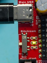
The LEDs besides the switch show the current image selected as well for confirmation. We recommend using Slot 2 (the middle setting), leaving Slot 1 as the test image we shipped.
In case you have trouble with the board, you can quickly switch to Slot 1 to confirm the LCD, LEDs, and similar are all functioning correctly. However there is no problem to overwrite any of the slots, the default image can easily be copied back if you want later.
Drag & Drop Programming
To program the Sonata bitstream:
- Download the bitstream from our releases
- Select slot 2 using switch SW3 (
Bitstream) - Plug in Sonata board. You should see a SONATA drive (see troubleshooting section if unsure).
- Drag the updated
.bitfile and wait for the copy to complete (on Linux note the copy command may return immediately, so you need to wait until it's done.) - The board should automatically restart once the image is copied over. You should see the
FPGA ConfigLED come on:
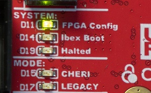
This indicates the FPGA configuration succeeded. This LED should stay on. You should also see the Ibex Boot LED come on indicating the processor core has booted.
The
FPGA ConfigLED reflects the state of the FPGADONEpin. If this LED is not on your board will not work, as there is no logic (core) loaded, or it has become corrupted. This is true even if you are not building Sonata designs but using the board as a general-purpose FPGA board. See troubleshooting below if this LED does not come on, or appears to only come on briefly.
Here is the commands you'd need to do all of that, assuming Sonata was already plugged in and has been mounted at /media/sonata
wget THEBESTURL.COM/lowrisc_sonata_system_0.bit
cp lowrisc_sonata_system_0.bit /media/sonata/.
Many Linux desktop distributions will automount if you open the drive via the graphical interface, so you may find it easier to do this from your Linux desktop, which 2024 is certainly the year of.
Programming on Power Cycle
Once the copy completes (it can take from 15-120 seconds), you should see the device reboot and the Ibex boot LED come on as mentioned. If you unplug & replug the USB cable, it will also reprogram the FPGA. The bitstream is stored on FLASH memory on the Sonata board.
Troubleshooting
Sonata Mass Storage Drive Issues
The Sonata board when plugged in should show a mass storage drive with these files:
LOG.TXT
OPTIONS.TXT
README.TXT
If the board has a RPI loader, visible because you'll see the file INFO_UF2.txt with the contents Model: Raspberry Pi RP2, you may need to reload the RP2040 as described in the Sonata Board Updating Firmware section. This could
be because the RPI Boot button was held down when plugging in the board.
The Sonata board will print status and messages to the LOG.TXT which can be helpful for debugging. It should show the status of valid-looking bitstreams:
CRIT: FW_VER 0.1.2
INFO: No bitstream in slot 0
INFO: No bitstream in slot 1
INFO: No bitstream in slot 2
INFO: Using slot 2
INFO: No bitstream in flash @ 1400000
FPGA Config Led not coming on
If the FPGA Config LED is not coming on, this could indicate the bitstream was designed for a different FPGA, or some other hardware issue. This should be troubleshooted with the OpenFPGALoader utility as described further down this page.
Ibex Boot LED not coming on
If the FPGA Config LED is on but the Ibex Boot LED is not, it may be that you have programmed (or selected) a different bitstream than one that runs the CHERIoT demo. Try reloading the bitstream, and try power cycling the device.
Device Rebooting During/After Programming (No Serial Activity)
The Sonata board takes a fair amount of power (>500mA) from the USB interface, and should be connected via USB-C. Typically it is close enough to the USB 2.0 limits that it will work with the adapter most of the time, but if you are having reliability issues we recommend trying a different computer, ideally one with a USB-C port.
If you use a recent openFPGALoader build from at least May 25, 2024 you can print the min/max VCCINT ranges. To do this, simply run:
openFPGALoader -c ft4232 -X
This will print several XADC values, pay careful attention to minvccint:
{"temp": 39.9061,
    "maxtemp": 40.3194,
    "mintemp": 25.9852,
"raw":  {"0": 40684, "1": 21949, "2": 39270, "3": 0, "4": 0, "5": 0, "6": 21948, "7": 0},
"vccint": 1.00415,
   "maxvccint": 1.00635,
   "minvccint": 1.00195,
"vccaux": 1.79663,
   "maxvccaux": 1.79883,
   "minvccaux": 1.79517,
}
The minvccint and maxvccint should be fairly close as shown here. Larger ranges indicate possible ringing, or a minvccint near or below 0.95V indicates a brown-out. You can compare the results of loading a different bitstream to see what is normal for your board.
See note below about if you get permissions error running openFPGALoader.
FPGA Programming via USB/JTAG
If for some reason the mass storage programming isn't working, you can also use the built-in FTDI JTAG programming. This requires the setup described in FPGA Programming to build openFPGALoader. Once built, you simply run:
openFPGALoader -c ft4232 sonata_top.bit
Note this requires the udev setup described in FPGA Programming. If you are lazy you can just run the command as root instead (not recommended, but can be helpful for troubleshooting on VMs):
sudo openFPGALoader -c ft4232 sonata_top.bit
You can also check if the flag --read-register STAT is available (newer than 0.12.2 is needed) which will print detailed information about the configuration status with a recent version of openFPGALoader. This is especially helpful if you are trying to understand why the DONE LED is not coming on:
CRC Error      No CRC error
Part Secured   0
MMCM lock      1
DCI match      1
EOS            0
GTS CFG B      0
GWE            0
GHIGH B        0
MODE           7
INIT Complete  1
INIT B         0
Release Done   0
Done           0
ID Error       ID error
DEC Error      0
XADC Over temp 0
STARTUP State  0
Reserved       0
BUS Width      x1
Reserved       8
Setting up the Toolchain for Software Development
All the special CHERIoT goodness comes with its own compiler that understands how to use it. For this reason you'll need to build a special toolchain from source. Luckily, it should be easy if you follow our simple instructions.
If building on Windows, the following instructions have also been confirmed to work with WSL2 with the exception of edalize and fusesoc,
which are not required for software development.
Nix Setup
We recommend using Nix for your setup. You can find instructions on how to do this in the Sonata software repository. This also includes a GitHub Codespaces that sets a whole environment up for you in the browser.
Manual Setup
Sonata Setup
git clone https://github.com/lowRISC/sonata-system
cd sonata-system

# Setup python venv
python3 -m venv .venv
source .venv/bin/activate

# Install python requirements
pip3 install -r python-requirements.txt
This installs requirements for both software and FPGA development. You may get errors on
edalizeandfusesoc-- don't panic, you don't need those for software. Just ignore the errors, you should see the rest of the packages installed successfully.
In the future, if you dare close this terminal, you'll need to do this before building Sonata examples:
cd sonata-system
source .venv/bin/activate
Building Toolchain
To build the toolchain, you'll need:
- clang
- ninja-build
- lld (llvm linker)
- cmake
On Ubuntu (including WSL), you can install them with:
sudo apt get install clang ninja-build lld cmake
HINT: You can see all the commands used to setup the test running in the CI YAML file. This provides a set of commands that is tested on each commit, in case you are having trouble building anything and want to see the expected output.
Build the toolchain with (again be sure this is in the .venv terminal):
git clone --depth 1 https://github.com/CHERIoT-Platform/llvm-project cheriot-llvm
cd cheriot-llvm
git checkout cheriot
# Create build directory
export LLVM_PATH=$(pwd)
mkdir -p builds/cheriot-llvm
cd builds/cheriot-llvm
# Build the toolchain
cmake ${LLVM_PATH}/llvm -DCMAKE_BUILD_TYPE=Release -DLLVM_ENABLE_PROJECTS="clang;clang-tools-extra;lld" -DCMAKE_INSTALL_PREFIX=install -DLLVM_ENABLE_UNWIND_TABLES=NO -DLLVM_TARGETS_TO_BUILD=RISCV -DLLVM_DISTRIBUTION_COMPONENTS="clang;clangd;lld;llvm-objdump;llvm-objcopy" -G Ninja
export NINJA_STATUS='%p [%f:%s/%t] %o/s, %es '
ninja install-distribution
NOTE: Currently the WSL2 build is broken and requires a patch applied as follows:
wget https://github.com/llvm/llvm-project/commit/4ad9ec8a328ccb3b836c993bba954366f05b2fd4.patch
git am < 4ad9ec8a328ccb3b836c993bba954366f05b2fd4.patch
Note the checkout and build will take some time, and the build process may have limited output during some steps.
This should put the binaries in a bin subdirectory of your build folder (the builds/cheriot-llvm folder you made).
With the CHERIoT/LLVM toolchain built, you can now continue to setup the examples and build them.
Building Examples
The following contains some simple examples you can build for the Sonata board. Once you've got these builds working, you can easily add more features to the example code.
Using our template
Please go to the Sonata software repository and build a full application from there. Inside your setup you should simply be able to build it like this:
git clone --recurse-submodule \
    https://github.com/lowRISC/sonata-software.git
cd sonata-software
xmake config --board=sonata
xmake build
After running this you should see the build run to completion and report success, the critical lines indicating a successful build are (note output size may differ):
Converted to uf2, output size: 74752, start address: 0x101000
Wrote 74752 bytes to build/cheriot/cheriot/release/sonata_simple_demo.uf2
[100%]: build ok, spent 6.827s
You can drag and drop this UF2 file into the SONATA drive to program the firmware.
Baremetal examples
This is only for advanced users. If you want to build the baremetal examples in the Sonata repo you can follow these instructions.
Additional Toolchain Setup
Besides the compiler, there are a few more features the example code depends on:
SRecord Tools
The makefile assumes srecord tools, which you can install with:
sudo apt install srecord
CHERIoT RTOS SDK Installation
You will need a copy of CHERIoT RTOS for this section.
On Windows you may need to set git config --global core.symlinks true before cloning the repository.
Clone the repository somewhere, not into the root of the sonata-system directory, but at the same level as sonata-system:
cd ..
git clone --recurse https://github.com/microsoft/cheriot-rtos.git
IMPORTANT: Set these two environmental variables. The first should point to the llvm build you did in the previous part,
and the second should point to the cheriot-rtos repo you just checked out:
export CHERIOT_LLVM_BIN=/path/to/cheriot-llvm/bin
export CHERIOT_RTOS_SDK=/path/to/cheriot-rtos/sdk
WARNING: The path to
/path/to/cheriot-llvm/binshould point to the build directory you created, not just the root checked outcheriot-llvmdirectory. The path will look something like:~/llvm-tools/cheriot-llvm/builds/cheriot-llvm/bin
The following assume you have run the source .venv/bin/activate command in the terminal you are using, and you are
currently at the root directory of your local sonata-system git repository.
Building Baremetal Examples
TODO: We should tell them where to get the SW. And especially point out it must match the bitstream version again (all downloaded at one point).
TODO: These environmental variables don't seem to be used by CMAKE but would need to be based. So these instructions are broken but kept as a starting point.
To build, run the following from the root of the directory which will build the examples:
cmake -B sw/cheri/build -S sw/cheri
cmake --build sw/cheri/build
The build output is put in the sw/cheri/build directory.
Two files of interest are created for each target: an ELF file which has no extension and a *.vmem file. The
*.vmem file can be used to load directly into the FPGA bitstream, described in more detail on the Programming the Sonata Software page.
If you get an error that
CMake will not be able to correctly generate this project., check back in the list to see if you see an error within the output similar toclang: error: unknown argument: '-mxcheri-rvc'. If this happens it means the wrong (non-CHERIoT) compiler was used. Check back to see what compiler is being used.
Loading software onto the FPGA
You can load software onto the FPGA over USB (JTAG) using:
./util/mem_helper.sh load_program -e sw/cheri/build/tests/spi_test
There are actually four different ways of loading the program - we normally use JTAG for development, but you can also program it into the serial flash device on the board. See the page Programming the Sonata Software.
Developer Guide
The Sonata architecture comprises a number of components:
- Physical board architecture: This is the board that hosts the FPGA (field programmable gate array), all other components, headers and interfaces.
- FPGA configuration architecture: It defines everything we are using a hardware description language for. This includes hardware IP blocks and bus architecture.
- Software architecture: This includes toolchain, operating system and applications.
Before we go into the architecture of the system, it is good to understand the use cases that we are envisioning, so that we can derive our architectural requirements from that.
Use cases and requirements
The Sonata is meant to be used by academics and industry users who are interested in experimenting with CHERIoT in embedded and IoT applications. This is the main reason why we are building a custom FPGA board so that we can make the platform easily usable. We also need the board to be as affordable as possible while still being performant and usable.
This ease of use comes in handy for classroom and demonstration use cases, for which we think this board will come in quite handy. In the classroom, it is also pertinent that we have a debuggable system.
Because we are focussing on embedded and IoT applications, we need to ensure connectivity. This includes being connectable to standard peripherals as well as being extendable with functionality required for niche use-cases.
The other major benefit of creating a custom board is that we can highlight CHERIoT specific features. We envision users of this board to want to show off and experiment with the new CHERIoT technology. If they are using the board as a demonstrator they will want to show off the prowess of CHERI, and if they are experimenting with the board they will want CHERI to be visible.
Like most physical boards, it is nice for it to be as interactive as possible. This means being able to accept user input and respond to them visibly and in an interactable way.
Beyond the physical Sonata board, we expect the soft design that is used to configure the FPGA to also be integrable into a bigger design. For example, we envision it being connected to OpenTitan Earl Grey through a bridge interface.
In short, these are our general requirements:
- Usable
- Affordable
- Debuggable
- Connectable
- Extendable
- CHERI visible
- Interactive
- Integrable
Detailed specifications
Toolchain
The toolchain will build on top of the work already done on CHERIoT, which uses a fork of LLVM. Through Sonata, we are not proposing any changes to the CHERIoT instruction set. We may need some changes to allow code to be stored in memory that does not have associated tags.
The toolchain for software development was described in the Getting Started section. If these instructions ever go out of date, you should be able to find the up to date instructions to build the toolchain from the CI YAML file.
Applications
Especially for the usable and CHERI-visible requirements, it is important that we have a set of demonstration applications. One demonstration application is cycling through each of the CHERIoT exception types with code snippets showing what went wrong. We can show what happens when CHERI is enabled and when it is disabled. We will provide at least some of these applications in bare-metal mode where they do not need an operating system.
Operating system
The CHERIoT RTOS work will need some reworking in terms of memory layout and drivers to work on the Sonata system.
FPGA (Soft-Core) architecture
The toolchain for FPGA (hardware/gateware) development is described in the FPGA Development section.
PCB architecture
This is described in the Board documentation.
Software Programming
There are four ways of programming the software:
-
You can use the flash storage on the Sonata board. This does not require special tools and allows an image to come online automatically at boot.
-
You can use OpenOCD to program the image onto RAM and then run this image. This is typically used during development.
-
You can use the CHERIoT serial bootloader. This loads the image into RAM on the CHERIoT system and then runs the image.
-
You can 'splice' the software into the FPGA image. This provides a single 'bitstream' including both hardware definition and software. This can be helpful for making system images that come alive as soon as possible after boot.
Flash Programming
OpenOCD/JTAG Programming
Serial Bootloader
Will this still be supported?
Splicing into FPGA Image
Reference Manual for Sonata Core
In a classical microcontroller, you would have a core along with the peripherals around the core. On the Sonata system this is all part of an open-source FPGA design, which allows you to modify the core to add new features (and for us to add updates to your core without needing you to desolder your main IC!).
This also means you can customize your design. You may want to have a different number of UARTs or SPI blocks for example. This document describes the base configuration, but you can
The FPGA image is parameterizable to enable custom setups. It should be easy, for example, to change the number of UART, SPI and I2C instances. We will provide pre-built images for common configurations.
Interoperate
For the interoperable requirement, we need to make sure our hardware design can interact with that of OpenTitan Earl Grey. Since OpenTitan Earl Grey uses a TileLink Uncached Lightweight (TL-UL) bus, we use the same in the Sonata system to ease designing a bridge interface.
Hardware IP blocks
To support all the peripherals that are on the FPGA boards, we need corresponding hardware IP blocks for Ibex to be able to interact with them:
- I2C for QWIIC
- SPI for the LCD screen and ethernet
- GPIO for buttons and LEDs
- HyperRAM controller
There might be other IP blocks necessary for interacting with headers such as an analogue to digital converter. We also need some modifications to CHERIoT Ibex, which are detailed in its own page.
Wherever possible, we reuse existing, high-quality, open-source hardware IP blocks that are fit for purpose.
Memory layout
For all registers in this section, the functionality is mapped onto the least significant bits of registers and each register is 32 bits wide.
| Base address | Size | Functionality |
|---|---|---|
| 0x0010_0000 | 256 KiB | Internal SRAM |
| 0x3000_0000 | 4 KiB | Revocation tags |
| 0x4000_0000 | 1 MiB | Tagged RAM |
| 0x4010_0000 | 7 MiB | Untagged RAM |
| 0x8000_0000 | 4 KiB | GPIO |
| 0x8000_1000 | 4 KiB | PWM |
| 0x8000_2000 | 4 KiB | DMA |
| 0x8000_3000 | 4 KiB | HyperRAM |
| 0x8000_4000 | 4 KiB | ADC |
| 0x8000_5000 | 4 KiB | Pinmux |
| 0x8004_0000 | 64 KiB | Timer |
| 0x8010_0000 | 1 MiB | UART |
| 0x8020_0000 | 1 MiB | I2C host |
| 0x8030_0000 | 1 MiB | SPI host |
| 0x8040_0000 | 1 MiB | USB device |
| 0x8800_0000 | 64 MiB | PLIC |
| 0xB000_0000 | 4 KiB | Debug module |
Clocking infrastructure
The whole system is driven by the same clock with the exception of the HyperRAM controller. Optionally the HyperRAM controller can be clocked higher than the rest of the chip. To accommodate this, we introduce a synchronization interface with primitive FIFOs.
Memory architecture
We have a few different types of memory in the Sonata system: FPGA SRAM, HyperRAM and flash. With CHERI we need to think about capability tags and revocation tags. Any memory that needs to contain capabilities must have one capability tag per 32 bits. Any memory that needs to be revocable must have one revocation tag per 32 bits.
Capability tags
All capability tags live in SRAM. All SRAM that is allocated for code and data will have corresponding capability tags. Any data stored to HyperRAM and flash are not expected to be tagged. Since capability tags are out of band information and do not need to be memory mapped, we can store these within the error correction bits that are available on the FPGA's memory.
We envision that code can live in HyperRAM with an instruction cache for improved performance. However, this does require code to be able to live in untagged memory. This should be fine as CHERI capabilities are derived and manipulated at runtime, but does require toolchain changes to LLVM and the corresponding RTOS (see software architecture).
Revocation tags
Revocation tags are essential in providing temporal memory safety in CHERI. This only covers a subset of memory that is likely to be used by the heap. Setting the revocation bit effectively stops any capability with that base address from being loaded from memory. This is a temporary step as the revocation engine scans through memory to invalidate all capabilities to this address. Once the complete memory is scanned, the revocation bit can be unset and the memory can be reused.
In Sonata, the revocation tags only cover a subset of mapped memory. They should apply to memory regions that are most likely to be used as heap, it is likely this will cover all of internal SRAM and some of HyperRAM. Unlike capability tags, revocation tags need to be memory mapped so the memory allocator can manipulate them.
In CHERIoT Ibex the size of memory allocated for this is defined by TSMapSize which indicates how many 32-bit words can be used for revocation bits.
The default value for this is 1,024, which corresponds to 8 KiB.
In CHERIoT Safe the size of the revocation tag memory is 16 KiB.
List of SRAM blocks
Here's a list of blocks by size that we need to allocate in SRAM. The XC7A35T has 100 blocks of 18 kilobit block RAM, see datasheet. In total that gives use 225 KiB of block RAM, but we may not efficiently map onto 18 kilobit blocks and thus lose some memory. The block RAM usage in the table below was calculated using Vivado 2023.2's block memory generator.
| Type | Size | Width | Depth | RAM Blocks |
|---|---|---|---|---|
| Internal memory | 128 KiB | 33 | 32,768 | 60 |
| Revocation tags | 16 KiB | 32 | 4,096 | 8 |
| RAM capability tags | 32 KiB | 32 | 8,192 | 15 |
| Instruction cache data | 4 KiB | 64 | 512 | 2 |
| Instruction cache tags | 1 KiB | 22 | 512 | 1 |
| Total | 181 KiB | 86 | ||
| Available | 225 KiB | 100 |
Ibex
For details on how Ibex works please look at the vendored in documentation. This page highlights the changes that we made to Ibex for the Sonata system.
The Sonata board has a CHERI enabled LED which is hard wired to the value of cheri_pmode_i of the Ibex core module.
Capability exception LEDs
In the CHERIoT specification there are number of capability exception codes.
The Sonata board has dedicated LEDs to indicate any of these errors.
When one of these exceptions is seen, it gets latched and displayed on the LED.
The LEDs do not clear once the exception is handled, instead software needs to clear these LEDs through a special CSR.
Custom M-mode CSR 0xBC0 is used for this purpose.
If bit 0 is set to 1 then hardware no longer drives the LEDs and software is in full control over the output.
The other bits positions correspond to the value of the exception code.
| Bit offset | Description |
|---|---|
| 24 | Permit access system registers violation |
| 22 | Permit store local capability violation |
| 21 | Permit store capability violation |
| 19 | Permit store violation |
| 18 | Permit load violation |
| 17 | Permit execute violation |
| 3 | Seal violation |
| 2 | Tag violation |
| 1 | Bounds violation |
| 0 | Disable |
Debug module
The debug module we use in Sonata supports the RISC-V debug specification. It also has support for CHERIoT so that capabilities can be viewed and manipulated.
GPIO
General purpose input and output is used for Ibex to interact with the buttons and switches on the board. It is also used to drive the LEDs on the board. There are also the GPIO pins of the various headers.
For the input this module provides a raw value as well as a debounced value. Debouncing is useful to avoid counting a single button press multiple times. For more information on contact bounce, see this Wikipedia page.
| Offset | Register |
|---|---|
| 0x00 | Output |
| 0x04 | Input |
| 0x08 | Debounced input |
| 0x0C | Debounce threshold |
| 0x10 | Raspberry pi header |
| 0x14 | Raspberry pi mask |
| 0x18 | Arduino shield header |
| 0x1C | Arduino shield mask |
Output
The output register displays the specified value onto the boards output.
| Bit offset | Description |
|---|---|
| 7-0 | LEDs |
In this case writing a one will turn an LED on and a zero will turn the LED off.
Input
Both input registers have the same bit mapping. The only difference between the registers is that the latter has debounced signals.
| Bit offset | Description |
|---|---|
| 13-9 | Joystick (left, down, up, right, press) |
| 8 | Button |
| 7-0 | DIP switches |
The input registers are used to interact with the joystick, the button and the DIP switches that are available on the Sonata board.
Debounce threshold
This register indicates how many clock cycles an input needs to be stable before it shows up on the output. The same threshold applies to all of the inputs.
| Bit offset | Description |
|---|---|
| 31-0 | Threshold |
Raspberry Pi header
The Raspberry Pi header has 26 GPIO pins, this register can read from and write to these pins. When writing, it only writes the bits for which the write mask has a one. The header and write mask registers have the same bit mapping.
| Bit offset | Description |
|---|---|
| 24 | GPIO 26 |
| ... | ... |
| 1 | GPIO 3 |
| 0 | GPIO 2 |
Arduino shield header
Arduino shield headers have 13 IO pins, this register can read from and write to these pins. When writing, it only writes the bits for which the write mask has a one. The header and the write mask registers have the same bit mapping.
| Bit offset | Description |
|---|---|
| 13 | IO 13 |
| ... | ... |
| 1 | IO 1 |
| 0 | IO 0 |
Universal asynchronous receiver/transmitter (UART)
The Sonata system uses the OpenTitan UART. You can find the register definitions here.
There are multiple UART instances in Sonata to connect to any of the following targets:
- USB
- RS-232
- mikroBUS
- Arduino shield
- Raspberry Pi hat
By default, Sonata includes 3 UART blocks, each with an offset of 0x1000 from each other.
Timer
The timer that we use in Sonata is based on the timer present in the Ibex repository. It is a simple memory mapped timer that sends an interrupt to Ibex after a specified amount of time. The time values in this block are 64 bits, which is why it has a high and a low register for each value.
| Offset | Register |
|---|---|
| 0x00 | Time low |
| 0x04 | Time high |
| 0x08 | Time compare low |
| 0x0C | Time compare high |
The processor can set the time by writing to the time low and high registers and then set a time compare value to compare to. Internally, the block increments the time by one each clock cycle. Once the internal counter has exceeded the compare value, it raises an interrupt with the Ibex.
Inter-integrated circuit (I2C) host
For the I2C block in Sonata, we use the OpenTitan IP.
We hardcode this block to be in host mode, so you can ignore the target functionality, including register ovrd, val, target_id, acqdata and txdata.
Other than those you can find the register definitions here.
The registers 0x00 - 0x10 are also not accessible.
The control register is just hardwired to be in host mode.
For Sonata, we include two I2C blocks.
The registers of the second I2C block can be accessed with and additional 0x1000 offset.
These can be connected to any of these I2C targets:
- Two for the QWIIC connectors.
- One for the mikroBUS.
- One for the Raspberry Pi hat.
- One for the Arduino shield.
Serial peripheral interface (SPI) host
The SPI in Sonata only has the capability to be a host. This is a simple hardware IP block that can transmit and receive bytes over SPI.
In Sonata, there are multiple uses for SPI:
- LCD screen
- Ethernet
- Flash
- Raspberry Pi hat
- Arduino shield
- mikroBUS
The current Sonata system configuration has two SPI instantiations, one for the LCD screen and one for Flash. The Sonata top-level will need modification to add more SPI blocks for other uses.
The offset for each of the blocks is shown below, with each additional block having a 0x1000 offset from the previous.
| SPI Instance | Offset (from SPI base) |
|---|---|
| Flash | 0x0 |
| LCD Screen | 0x1000 |
| Ethernet MAC | 0x2000 |
Overview
Each SPI block has a two 64 entry FIFOs one for transmit and one for receive.
To begin an SPI transaction write to the START register.
Bytes do not need to be immediately available in the transmit FIFO nor space available in the receive FIFO to begin the transaction.
The SPI block will only run the clock when its able to proceed.
Note that the CS pin is not handled by the SPI block and must be dealt with via GPIO and controlled with software.
Note Interrupts are not yet implemented
Register Table
| Name | Offset | Length | Description |
|---|---|---|---|
spi.INTR_STATE | 0x0 | 4 | Interrupt State Register |
spi.INTR_ENABLE | 0x4 | 4 | Interrupt Enable Register |
spi.INTR_TEST | 0x8 | 4 | Interrupt Test Register |
spi.CFG | 0xc | 4 | Configuration register. Controls how the SPI block transmits |
spi.CONTROL | 0x10 | 4 | Controls the operation of the SPI block. This register can |
spi.STATUS | 0x14 | 4 | Status information about the SPI block |
spi.START | 0x18 | 4 | When written begins an SPI operation. Writes are ignored when the |
spi.RX_FIFO | 0x1c | 4 | Data from the receive FIFO. When read the data is popped from the |
spi.TX_FIFO | 0x20 | 4 | Bytes written here are pushed to the transmit FIFO. If the FIFO |
INTR_STATE
Interrupt State Register
- Offset:
0x0 - Reset default:
0x0 - Reset mask:
0x1f
Fields
| Bits | Type | Reset | Name | Description |
|---|---|---|---|---|
| 31:5 | Reserved | |||
| 4 | rw1c | 0x0 | complete | On-going SPI operation has completed and the block is now idle |
| 3 | ro | 0x0 | tx_watermark | Transmit FIFO level is at or below watermark |
| 2 | ro | 0x0 | tx_empty | Transmit FIFO is empty |
| 1 | ro | 0x0 | rx_watermark | Receive FIFO level is at or above watermark |
| 0 | ro | 0x0 | rx_full | Receive FIFO is full |
INTR_ENABLE
Interrupt Enable Register
- Offset:
0x4 - Reset default:
0x0 - Reset mask:
0x1f
Fields
| Bits | Type | Reset | Name | Description |
|---|---|---|---|---|
| 31:5 | Reserved | |||
| 4 | rw | 0x0 | complete | Enable interrupt when INTR_STATE.complete is set. |
| 3 | rw | 0x0 | tx_watermark | Enable interrupt when INTR_STATE.tx_watermark is set. |
| 2 | rw | 0x0 | tx_empty | Enable interrupt when INTR_STATE.tx_empty is set. |
| 1 | rw | 0x0 | rx_watermark | Enable interrupt when INTR_STATE.rx_watermark is set. |
| 0 | rw | 0x0 | rx_full | Enable interrupt when INTR_STATE.rx_full is set. |
INTR_TEST
Interrupt Test Register
- Offset:
0x8 - Reset default:
0x0 - Reset mask:
0x1f
Fields
| Bits | Type | Reset | Name | Description |
|---|---|---|---|---|
| 31:5 | Reserved | |||
| 4 | wo | 0x0 | complete | Write 1 to force INTR_STATE.complete to 1. |
| 3 | wo | 0x0 | tx_watermark | Write 1 to force INTR_STATE.tx_watermark to 1. |
| 2 | wo | 0x0 | tx_empty | Write 1 to force INTR_STATE.tx_empty to 1. |
| 1 | wo | 0x0 | rx_watermark | Write 1 to force INTR_STATE.rx_watermark to 1. |
| 0 | wo | 0x0 | rx_full | Write 1 to force INTR_STATE.rx_full to 1. |
CFG
Configuration register. Controls how the SPI block transmits and receives data. This register can only be modified whilst the SPI block is idle.
- Offset:
0xc - Reset default:
0x20000000 - Reset mask:
0xe000ffff
Fields
| Bits | Type | Reset | Name |
|---|---|---|---|
| 31 | rw | 0x0 | CPOL |
| 30 | rw | 0x0 | CPHA |
| 29 | rw | 0x1 | MSB_FIRST |
| 28:16 | Reserved | ||
| 15:0 | rw | 0x0 | HALF_CLK_PERIOD |
CFG . CPOL
The polarity of the spi_clk signal. When CPOL is 0 clock is low when idle and the leading edge is positive. When CPOL is 1 clock is high when idle and the leading edge is negative
CFG . CPHA
The phase of the spi_clk signal. When CPHA is 0 data is sampled on the leading edge and changes on the trailing edge. The first data bit is immediately available before the first leading edge of the clock when transmission begins. When CPHA is 1 data is sampled on the trailing edge and change on the leading edge.
CFG . MSB_FIRST
When set the most significant bit (MSB) is the first bit sent and received with each byte
CFG . HALF_CLK_PERIOD
The length of a half period (i.e. positive edge to negative edge) of the SPI clock, measured in system clock cycles reduced by 1. At the standard Sonata 50 MHz system clock a value of 0 gives a 25 MHz SPI clock, a value of 1 gives a 12.5 MHz SPI clock, a value of 2 gives a 8.33 MHz SPI clock and so on.
CONTROL
Controls the operation of the SPI block. This register can only be modified whilst the SPI block is idle.
- Offset:
0x10 - Reset default:
0x0 - Reset mask:
0xfff
Fields
| Bits | Type | Reset | Name |
|---|---|---|---|
| 31:12 | Reserved | ||
| 11:8 | rw | 0x0 | RX_WATERMARK |
| 7:4 | rw | 0x0 | TX_WATERMARK |
| 3 | rw | 0x0 | RX_ENABLE |
| 2 | rw | 0x0 | TX_ENABLE |
| 1 | wo | 0x0 | RX_CLEAR |
| 0 | wo | 0x0 | TX_CLEAR |
CONTROL . RX_WATERMARK
The watermark level for the receive FIFO, depending on the value the interrupt will trigger at different points:
- 0: 1 or more items in the FIFO
- 1: 2 or more items in the FIFO
- 2: 4 or more items in the FIFO
- 3: 8 or more items in the FIFO
- 4: 16 or more items in the FIFO
- 5: 32 or more items in the FIFO
- 6: 56 or more items in the FIFO
CONTROL . TX_WATERMARK
The watermark level for the transmit FIFO, depending on the value the interrupt will trigger at different points:
- 0: 1 or fewer items in the FIFO
- 1: 2 or fewer items in the FIFO
- 2: 4 or fewer items in the FIFO
- 3: 8 or fewer items in the FIFO
- 4: 16 or fewer items in the FIFO
CONTROL . RX_ENABLE
When set incoming bits are written to the receive FIFO. When clear incoming bits are ignored.
CONTROL . TX_ENABLE
When set bytes from the transmit FIFO are sent. When clear the state of the outgoing spi_cipo is undefined whilst the SPI clock is running.
CONTROL . RX_CLEAR
Write 1 to clear the receive FIFO.
CONTROL . TX_CLEAR
Write 1 to clear the transmit FIFO.
STATUS
Status information about the SPI block
- Offset:
0x14 - Reset default:
0x0 - Reset mask:
0x7ffff
Fields
| Bits | Type | Reset | Name | Description |
|---|---|---|---|---|
| 31:19 | Reserved | |||
| 18 | ro | x | IDLE | When set the SPI block is idle and can accept a new start command. |
| 17 | ro | x | RX_FIFO_EMPTY | When set the receive FIFO is empty and any data read from it will be undefined. |
| 16 | ro | x | TX_FIFO_FULL | When set the transmit FIFO is full and any data written to it will be ignored. |
| 15:8 | ro | x | RX_FIFO_LEVEL | Number of items in the receive FIFO |
| 7:0 | ro | x | TX_FIFO_LEVEL | Number of items in the transmit FIFO |
START
When written begins an SPI operation. Writes are ignored when the SPI block is active.
- Offset:
0x18 - Reset default:
0x0 - Reset mask:
0x7ff
Fields
| Bits | Type | Reset | Name | Description |
|---|---|---|---|---|
| 31:11 | Reserved | |||
| 10:0 | wo | 0x0 | BYTE_COUNT | Number of bytes to receive/transmit in the SPI operation |
RX_FIFO
Data from the receive FIFO. When read the data is popped from the FIFO. If the FIFO is empty data read is undefined.
- Offset:
0x1c - Reset default:
0x0 - Reset mask:
0xff
Fields
| Bits | Type | Reset | Name | Description |
|---|---|---|---|---|
| 31:8 | Reserved | |||
| 7:0 | ro | x | DATA | Byte popped from the FIFO |
TX_FIFO
Bytes written here are pushed to the transmit FIFO. If the FIFO is full writes are ignored.
- Offset:
0x20 - Reset default:
0x0 - Reset mask:
0xff
Fields
| Bits | Type | Reset | Name | Description |
|---|---|---|---|---|
| 31:8 | Reserved | |||
| 7:0 | wo | 0x0 | DATA | Byte to push to the FIFO |
USB 2.0 device
The USB (Universal Serial Bus) device hardware IP block in Sonata is taken from the OpenTitan project. You can find the full documentation here.
Multiple USB devices are allowed to be instantiated at a 0x1000 offset from each other up to a maximum of 256 instantiations.
HyperRAM controller
HyperRAM is used as an alternative to flash. Compared to flash, HyperRAM has similar performance but it avoids the need for a quad-speed SPI controller to interact with the flash. The HyperRAM controller is the interface between the Sonata system and the actual chip.
| Offset | Register |
|---|---|
| 0x00 | Configuration 0 |
| 0x04 | Configuration 1 |
For details of what these configuration registers do please consult Section 9.4 and 9.5 of the datasheet.
Because the latency of accessing data memory through the HyperRAM will be quite slow, we introduce a fully-associated cache of a few words to improve performance. It is anticipated main data storage will be in SRAM with the HyperRAM storing small amounts of data interleaved with code so more significant caching is unnecessary.
Capability enabled RAM
The HyperRAM controller is also where the capability tags live for the tagged part of the RAM. In Sonata we allocate 32 KiB for capability tags for RAM which translates in to 1 MiB for tagged RAM.
Pulse width modulation (PWM)
Pulse width modulation allows you to create a block wave with a certain duty cycle. It is useful for use cases like dimming LEDs.
| Offset | Register |
|---|---|
| 0x00 | Enable |
| 0x10 | Config 0 |
| 0x14 | Config 1 |
| 0x18 | Config 2 |
| 0x1C | Config 3 |
| 0x20 | Config 4 |
| 0x24 | Config 5 |
| 0x28 | Config 6 |
| 0x2C | Config 7 |
Enable
This has a bit per PWM on whether to enable it or not.
| Bit offset | Description |
|---|---|
| 7 | Enable for PWM 7 |
| ... | ... |
| 1 | Enable for PWM 1 |
| 0 | Enable for PWM 0 |
Config
For each output, there is a register defining the pulse width and how long the complete wave is (indicated by the counter value).
| Bit offset | Description |
|---|---|
| 31-16 | Counter |
| 15-0 | Pulse width |
Platform-level interrupt controller (PLIC)
The PLIC is a RISC-V interrupt controller and specifically we are using OpenTitan's interrupt controller.
Please find more details in the official specification.
Part of these details are is the memory map, which shows all registers from the base until base + 0x3FFFFFC.
Not all of these registers are mapped, most importantly we only have one core, so only one context (context 0).
In terms of interrupts, the exact mapping of sources to interrupts will be published here at a later point. There are a number of considerations.
- The following blocks have interrupts: timer, UART, I2C, SPI, ...
- There are multiple UART, I2C and SPI blocks in the system.
- Some blocks have multiple interrupts.
FPGA development
This page is only for if you want to make changes to the RTL of the bitstream. In most cases you can just use the standard bitstream published in the releases.
Dependencies
FPGA Build
The Sonata bitstream is generated using Vivado.
Bitstream
To build the bitstream, make sure to build the software to create the correct SRAM image. Then run this command:
fusesoc --cores-root=. run --target=synth --setup --build lowrisc:sonata:system
You can also manually set the initial value of the SRAM, for example:
fusesoc --cores-root=. run --target=synth --setup --build lowrisc:sonata:system --SRAMInitFile=$PWD/sw/cheri/build/tests/uart_check.vmem
FPGA Programming
Drag & Drop Programming
The easiest way to program the FPGA is to use the built-in programming feature. This reads a .bit file you drag onto the USB drive that comes up when the USB is plugged in, and will program it into the FPGA. This will also save it to SPI flash in one of the three "Slots", and will automatically reprogram on board power-on.
Using this drag & drop programming is the suggested way of updating the board with "normal" Sonata core images. For development it's suggested to use the JTAG programmer, as it will be much faster and avoids lots of writes to the SPI flash.
JTAG Programming Using On-Board FTDI Chip
The Sonata board includes a FTDI chip that can program the FPGA. This also allows usage inside of Vivado to access features such as Integrated Logic Anlayzer (ILA) blocks.
On the backside of the board, confirm switches SW1 are all set to ON as shown in this photo (this was the state the board is shipped in, so if you haven't touched the switches it should still be in that state):
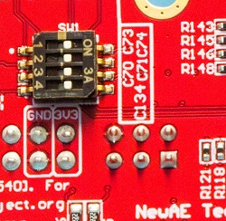
The switches in the "off" state will isolate the FTDI and allow you to use an external JTAG probe (such as Xilinx Platform Cable USB II).
USB rules for Linux
To allow openFPGAloader to program our device, add the following rules:
sudo su
cat <<EOF > /etc/udev/rules.d/99-openfpgaloader.rules
# Copy this file to /etc/udev/rules.d/

ACTION!="add|change", GOTO="openfpgaloader_rules_end"

# gpiochip subsystem
SUBSYSTEM=="gpio", MODE="0664", GROUP="plugdev", TAG+="uaccess"

SUBSYSTEM!="usb|tty|hidraw", GOTO="openfpgaloader_rules_end"

# Original FT232/FT245 VID:PID
ATTRS{idVendor}=="0403", ATTRS{idProduct}=="6001", MODE="664", GROUP="plugdev", TAG+="uaccess"

# Original FT2232 VID:PID
ATTRS{idVendor}=="0403", ATTRS{idProduct}=="6010", MODE="664", GROUP="plugdev", TAG+="uaccess"

# Original FT4232 VID:PID
ATTRS{idVendor}=="0403", ATTRS{idProduct}=="6011", MODE="664", GROUP="plugdev", TAG+="uaccess"

# Original FT232H VID:PID
ATTRS{idVendor}=="0403", ATTRS{idProduct}=="6014", MODE="664", GROUP="plugdev", TAG+="uaccess"

# Original FT231X VID:PID
ATTRS{idVendor}=="0403", ATTRS{idProduct}=="6015", MODE="664", GROUP="plugdev", TAG+="uaccess"

# anlogic cable
ATTRS{idVendor}=="0547", ATTRS{idProduct}=="1002", MODE="664", GROUP="plugdev", TAG+="uaccess"

# altera usb-blaster
ATTRS{idVendor}=="09fb", ATTRS{idProduct}=="6001", MODE="664", GROUP="plugdev", TAG+="uaccess"
ATTRS{idVendor}=="09fb", ATTRS{idProduct}=="6002", MODE="664", GROUP="plugdev", TAG+="uaccess"
ATTRS{idVendor}=="09fb", ATTRS{idProduct}=="6003", MODE="664", GROUP="plugdev", TAG+="uaccess"

# altera usb-blasterII - uninitialized
ATTRS{idVendor}=="09fb", ATTRS{idProduct}=="6810", MODE="664", GROUP="plugdev", TAG+="uaccess"
# altera usb-blasterII - initialized
ATTRS{idVendor}=="09fb", ATTRS{idProduct}=="6010", MODE="664", GROUP="plugdev", TAG+="uaccess"

# dirtyJTAG
ATTRS{idVendor}=="1209", ATTRS{idProduct}=="c0ca", MODE="664", GROUP="plugdev", TAG+="uaccess"

# Jlink
ATTRS{idVendor}=="1366", ATTRS{idProduct}=="0105", MODE="664", GROUP="plugdev", TAG+="uaccess"

# NXP LPC-Link2
ATTRS{idVendor}=="1fc9", ATTRS{idProduct}=="0090", MODE="664", GROUP="plugdev", TAG+="uaccess"

# NXP ARM mbed
ATTRS{idVendor}=="0d28", ATTRS{idProduct}=="0204", MODE="664", GROUP="plugdev", TAG+="uaccess"

# icebreaker bitsy
ATTRS{idVendor}=="1d50", ATTRS{idProduct}=="6146", MODE="664", GROUP="plugdev", TAG+="uaccess"

# orbtrace-mini dfu
ATTRS{idVendor}=="1209", ATTRS{idProduct}=="3442", MODE="664", GROUP="plugdev", TAG+="uaccess"

LABEL="openfpgaloader_rules_end"

EOF

exit
Run the following to reload the rules:
sudo udevadm control --reload-rules
sudo udevadm trigger
Add user to plugdev group:
sudo usermod -a $USER -G plugdev
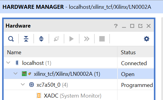
Programming with openFPGALoader (Linux/MacOS)
Programming the FPGA:
openFPGALoader -c ft4232 build/lowrisc_sonata_system_0/synth-vivado/lowrisc_sonata_system_0.bit
You can also check if the flag --read-register STAT is available (newer than 0.12.2 is needed) which will print detailed information about the configuration status with a recent version of openFPGALoader. This is especially helpful if you are trying to understand why the DONE LED is not coming on:
$ openFPGALoader -c ft4232 build/lowrisc_sonata_system_0/synth-vivado/lowrisc_sonata_system_0.bit --read-register STAT

CRC Error      No CRC error
Part Secured   0
MMCM lock      1
DCI match      1
EOS            0
GTS CFG B      0
GWE            0
GHIGH B        0
MODE           7
INIT Complete  1
INIT B         0
Release Done   0
Done           0
ID Error       ID error
DEC Error      0
XADC Over temp 0
STARTUP State  0
Reserved       0
BUS Width      x1
Reserved       8
In this example there is an ID error that means the wrong bitstream was used (e.g., built for an A35, A75, or A100 and not for the A50).
Vivado (Windows)
The FTDI on the board is setup to work with Vivado, and should be detected on a recent version of Vivado (tested with 2023.2), older versions will not work. It also doesn't seem to currently work on Linux, although it "should" be supported according to Xilinx.
Reloading the FTDI Chip
The FT4232H on the board needs to be programmed by Vivado to work within Vivado. This is done from the TCL Console within Vivado.
With a blank FTDI chip, you would run the command:
program_ftdi -write -ftdi=FT4232H -serial LNXXXX -board "Sonata"
Where LNXXXX is the serial number on the sticker of the board (the serial number is optional, but with a serial number set the related
COM ports will always come up on Windows with the same COM port number, which can be helpful).
This will fail if the FTDI chip was programmed before. If you need to erase an FTDI chip, you would run the command:
program_ftdi -erase
The
program_ftdicommand can also be run from the system command prompt with the Vivado path setup.
JTAG Programming Using External Probe
If using an external probe, you need to connect to P10, labeled FPGA JTAG. This is normally done with flying wire leads.
Be sure you set all of the 4-position DIP switches within SW1 to OFF on the bottom of the board, otherwise your external JTAG probe will be fighting with the FTDI lines. This will cause unreliable operation.
Simulation
The Sonata simulation environment uses Verilator.
Building
Use the following FuseSoC command to build the simulator binary:
fusesoc --cores-root=. run --target=sim --tool=verilator --setup --build lowrisc:sonata:system
To enable tracing append, --verilator_options='+define+RVFI' to the command above.
Running
Running the simulator can be accomplished with the following command, where you can change the meminit argument to a different program if you wish:
./build/lowrisc_sonata_system_0/sim-verilator/Vtop_verilator -t --meminit=ram,./sw/cheri/cheri_sanity/boot.elf
I recommend that you make the following change to the sanity check to see quicker changes in simulation:
diff --git a/sw/cheri/cheri_sanity/boot.cc b/sw/cheri/cheri_sanity/boot.cc
index 547abb3..7f7781d 100644
--- a/sw/cheri/cheri_sanity/boot.cc
+++ b/sw/cheri/cheri_sanity/boot.cc
@@ -32,7 +32,7 @@ extern "C" uint32_t rom_loader_entry(void *rwRoot)
        uint32_t switchValue = 0;
        while (true) {
                gpioValue ^= GPIO_VALUE;
-               for (int i = 0; i < 5000000; i++) {
+               for (int i = 0; i < 5; i++) {
                        switchValue = *((volatile uint32_t *) gpi);
                        switchValue <<= 4; // shift input onto LEDs and skipping LCD pins
                        *((volatile uint32_t *) gpo) = gpioValue ^ switchValue;
Debugging
If you want to look at the internal design in more details, you can explore the waveforms produced by the simulation using GTKWave:
gtkwave sim.fst data/pc_and_gpo.gtkw
Building Documentation
The documentation uses mdBook see the installation guide for further details on installation.
Once mdBook is installed the documentation can be built and viewed with:
mdbook serve --open
# Avoid FuseSoC using copied files in the book directory
touch book/FUSESOC_IGNORE
The second line can be ignored if you aren't building the FPGA bitstream (which uses fusesoc).
Windows Quick-Start
On Windows the easiest installation method is to copy the precompiled mdbook.exe available as a release on the previous link to the sonata-system root directory.
./mdbook.exe serve --open
Sonata Board Reference
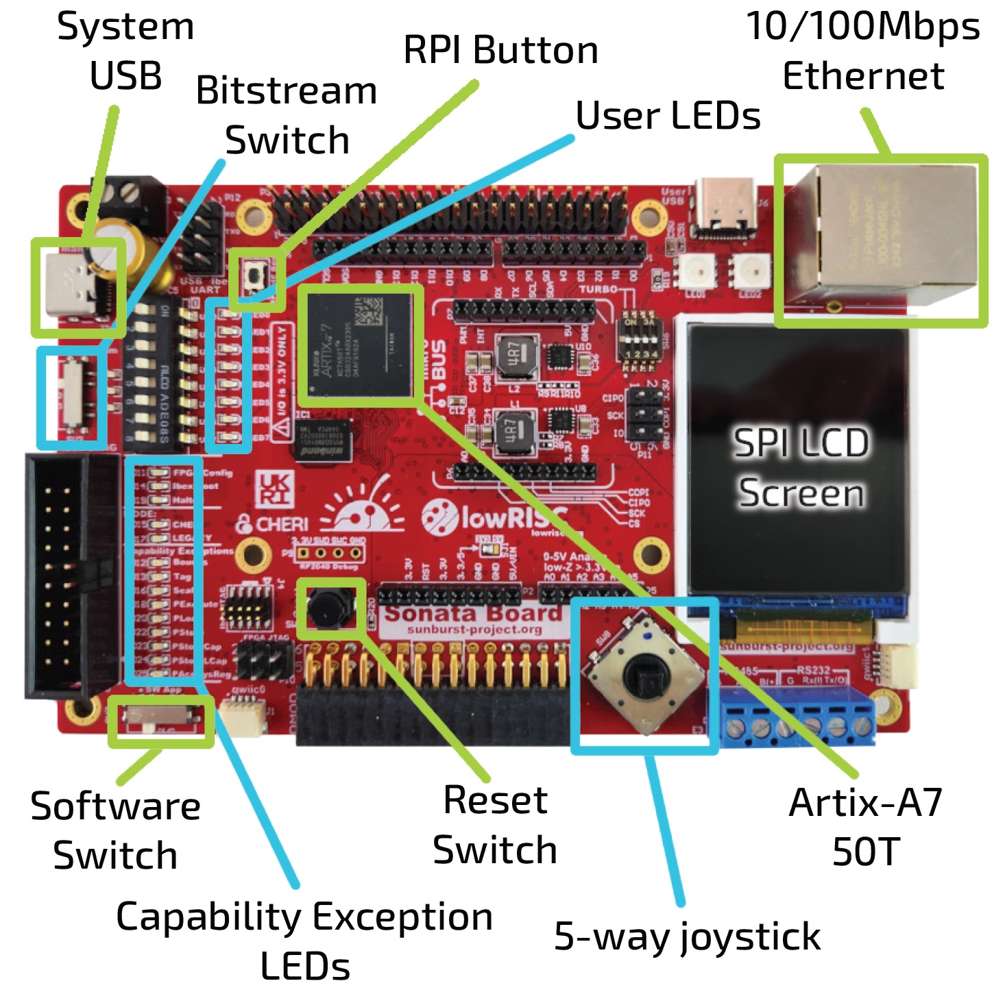
This section focusses on what needs to be physically present on the board and explicitly leaves the configuration of the FPGA and the software for other sections. The Sonata board has the features shown here:
Configuration
The 'usable' requirement makes it worth thinking well about configuration. We want to provide multiple bitstreams and software images that can be switched between on the board without having to reprogram it. This is why we have a switch for bitstream and a switch for software images.
For example, we could have a CHERI and non-CHERI bitstream both available on the board. For software, we can switch between demo applications, for example CHERI compartmentalization versus CHERI exceptions. Introducing these physical switches also fulfills the 'interactive' requirement.
To make multiple bitstreams available, we introduce a USB connector that looks like mass storage to a user, where multiple bitstreams can be stored and changed without hassle. There is an RP2040 on the board to manage these configurations.
Also part of this 'usable' requirement is to have enough memory to store the bitstreams and software. We introduce two separate flash chips for these purposes and a HyperRAM chip.
Peripherals
The 'connectable' requirement means that we need to introduce common peripherals on the board. After consultation with the community, we settled on the following list:
- Ethernet
- RS-232
- RS-485
- MicroSD
- ADC
Headers
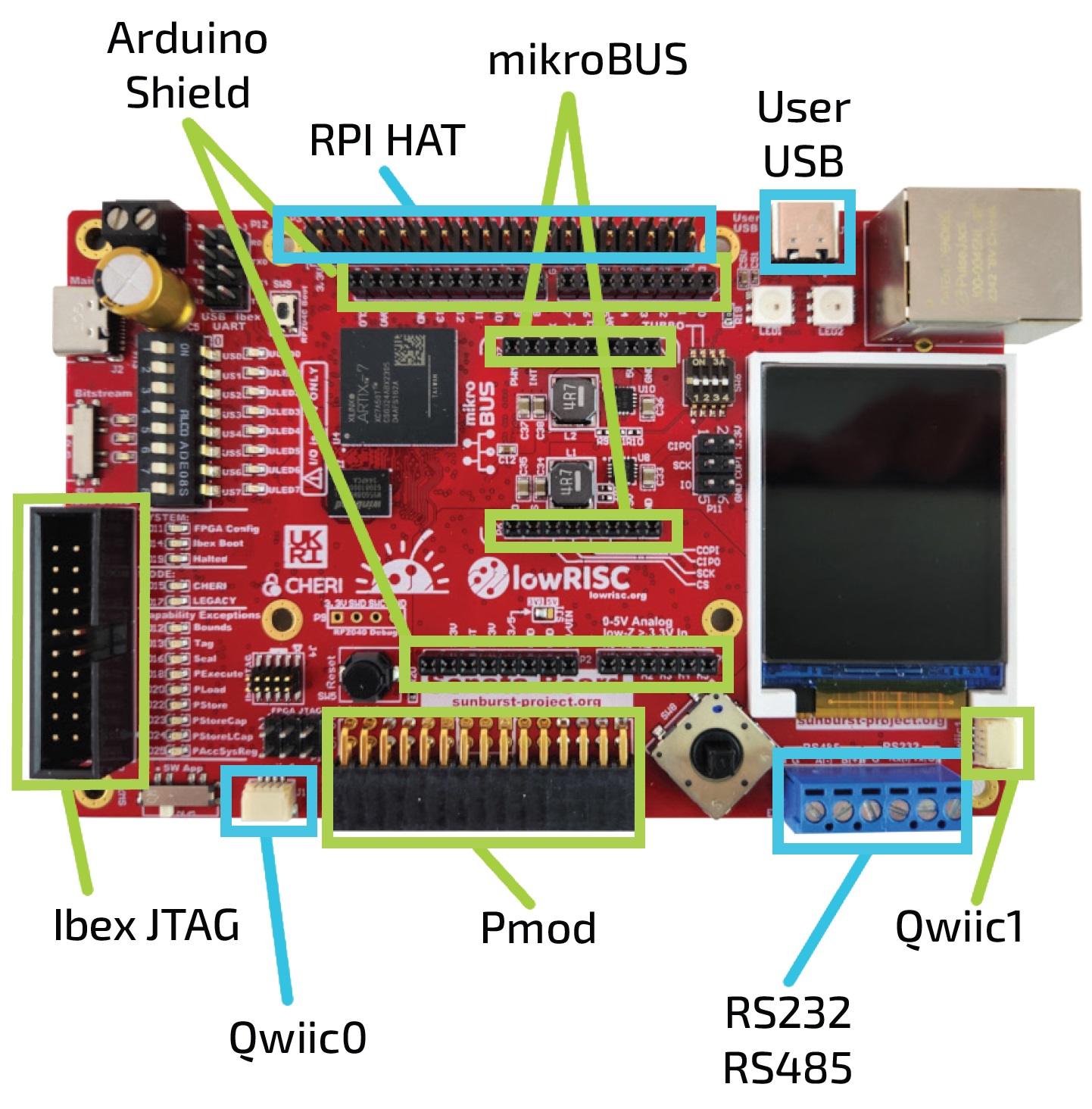
For both the 'connectable' and 'extendable' requirements, we provide a number of headers so that custom functionality can be added:
- Raspberry Pi header
- Arduino shield (only 3.3V versions supported)
- microBUS Click
- Sparkfun QWIIC
- PMOD
- 30-pin R/A header
Although, the FPGA pins can be used independently, due to the physical layout of the headers on the FPGA board, it is not possible to plug in Raspberry Pi, Arduino shield and MicroBus click headers simultaneously. You can still use them simultaneously with modified wiring.
The 2 PMODs and the R/A header cannot be used at the same time since they use the same pins. We don't expect this to be a problem as most applications should only need to use one expansion board.
Debug
For ease of use, we have one USB connector that can power the board as well as debug using JTAG and two virtual UARTs. This means that users only have to connect one cable. Besides the JTAG over USB, we provide external JTAG and UART headers to enable users to use different setups if they need to.
User interface
The user interface is where we address the 'CHERI-visible' and 'interactive' requirements. In terms of user input, we have:
- DIP switches
- Button
- Joystick
In terms of output, we have:
- LEDs
- LCD screen
- CHERI-specific capability exception LEDs
Affordable
In order to meet the 'affordable' requirement, we choose a low-end FPGA to reduce the costs. We choose a Xilinx Artix 7 FPGA because it has a typical amount of memory for embedded use-cases while being able to clock the design higher than similarly priced alternatives and being supported by many tools.
Technical details
If you want to know more details on what the actual design looks like, please have a look at NewAE's repository of the Sonata PCB.
This includes the entire design sources, available currently in Altium, with a KiCad version being released shortly.
Schematic Link
You can find a direct link to the schematics for your reading pleasure.
Default DIP switch settings
We recommend the following default state for the dipswitches:
- On the front:
- SW3 "Bitstream": 2
- SW7 "SW App": 1
- SW4 "US[0-7]": all set to off
- SW6 : all set to off
- On the back:
- SW1 : all set to on
- SW2 : 1-6 set to on and 7-8 set to off
RP2040 firmware
You can build new RP2040 firmware (or find release UF2 files) from the Sonata RP2040 repository.
With that UF2 file you can now update your firmware by holding down SW9, labelled "RP2040 Boot".
While holding this button plug your Sonata board in using the main USB.
A drive called RPI-RP2 should now appear which you can drag the UF2 file onto.